We pride oursalve being the expert specifically for
Laser Electron,Optics.
We will meet every needs with our extensive experience and technology.


- TOP
- >Business Overview
Business Overview
Information
The Semiconductor Equipment Group of Kobe Steel, Ltd. had committed the development and production of semiconductor evaluation equipment to LEO Business of Genesis Technology Corporation, a subsidiary of Kobe Steel, Ltd. However, on April 1, 2001, for realizing more effective business activities, LEO Business in KOBELCO RESEARCH INSTITUTE. INC. was newly established.
KOBELCO RESEARCH INSTITUTE, INC., a subsidiary of Kobe Steel, Ltd., is comprehensive testing and study company, as is introduced below. In addition to its mainstay services, Kobelco offers overall solutions through the LEO Business and we look forward to continuing our relationship with you.
Outline of KOBELCO RESEARCH INSTITUTE, INC.
| Name | KOBELCO RESEARCH INSTITUTE, INC. | |
|---|---|---|
| Headquarters | Head Office | Kokusai Kenko Kaihatsu Center 3F 1-5-1 Wakihamakaigandori, Chuo-ku, Kobe, HYOGO, 651-0073, JAPAN TEL : 81-78-272-5915 FAX : 81-78-265-3622 |
| Sales(Tokyo) | 5-9-12 Kitashinagawa, Shinagawa-ku, TOKYO, 141-8688, JAPAN TEL : 81-3-5739-5363 FAX : 81-3-5739-5371 |
|
| Sales(Kobe) | 5-5 Takatsuka-dai, 1-Chome, Nishi-ku, Kobe, HYOGO, 651-2271, JAPAN TEL : 81-78-992-2985 FAX : 81-78-992-2990 |
|
| Establishment | June 1979 | |
| Services | Material mechanical and physical property evaluation, Corrosion resistance evaluation, Corrosion trouble examination, Micro surface and fine area analysis study, Chemical analysis, Organic analysis, Physical analysis, Corrosion test, Property test, Strength test, Welding test, Environment measurement analysis and test, Spattering target materials, parts, test materials Semiconductor evaluation products (New: LEO Division) |
|
| Major customers | Kobe steel, Ltd., Kobe Steel Group companies, Public agencies, Power companies, Electric equipment companies, Automobile companies, Others | |
History of LEO Division
LEO Division of KOBELCO RESEARCH INSTITUTE, INC. carried on the business of LEO Giken, special group centered on Laser-Electro-Optics: LEO. KOBELCO has produced numerous products focusing on L-E-O technologies such as lifetime measuring unit, ion dose monitor, edge profile monitor and wafer sorter, and has been satisfying customers' needs with high technology and accumulated experiences. We pride ourselves on placing our "First priority on customers".
| 1976.04 | LEO Giken was established mainly by members of laser study sector of Ushio INC. |
|---|---|
| 1976.10 | Laser print image processor was developed for the first time in Japan. |
| 1977.03 | Laser bar code reading system was developed. |
| 1980.01 | Lifetime measuring system for silicon wafer was developed. |
| 1981.09 | Spatial data transfer system using laser was developed. |
| 1982.10 | Plane scanning laser imaging unit was developed. |
| 1984.05 | Silicon wafer resistivity and thickness auto measuring system was developed. |
| 1985.05 | Color image scanner was developed. |
| 1985.12 | Silicon wafer defect scanner was developed. |
| 1987.07 | Kobe Steel, Ltd. took an equity share in LEO Giken. |
| 1991.03 | Highly-precise, high-speed full-auto lifetime measuring system LTA-550 was developed. |
| 1993.01 | Crystallization defect evaluation system PA300 was developed. |
| 1993.04 | Edge shape measuring system for silicon wafer, wafer auto handling unit were developed. |
| 1993.12 | Variiable injection type lifetime measuring system LTA-700 was developed. |
| 1994.10 | TCP testing system was developed. |
| 1994.11 | Lead frame defect tester LF1-100 was developed. |
| 1994.12 | Ion implantation evaluation system PA400 was developed. |
| 1995.01 | Kobe Steel, Ltd. succeeded the business of LEO Giken. |
| 1995.12 | Sales of wafer ID sorter was started. |
| 1996.12 | Lifetime measuring system with epi wafer evaluation function was developed. |
| 1997.01 | Charge-up damage evaluation service was started. |
| 1997.12 | Edge chipping tester was developed. |
| 1997.01 | Probe card tester was developed. |
| 1998.07 | Lifetime measuring unit with iron density measuring function was developed. |
| 1998.12 | Color edge microscope was developed. |
| 1999.10 | Wafer batch transfer system was developed. |
| 2000.07 | Simple Bow/Warp measuring system was developed. |
| 2000.08 | Makyo system for 300mm wafer was developed. |
| 2001.04 | KOBELCO RESEARCH INSTITUTE, INC. newly established LEO Division, and succeeded the business. |
| 2003.02 | Low-Temperature Poly-Silicon(LTPS)crystallization evaluation system for flat panel display was developed. |
| 2003.09 | Edge Roll Off measurement system was developed. |
| 2006.12 | GBIR measuring system Series LGW was developed. |
| 2007.02 | Wafer surface roughness measuring systrem was developed. |
| 2008.07 | Precision diameter measurement device, notch edge profile monitor was developed. |
| 2010.06 | Edge profile monitor for sapphire, SiC was developed. |
| 2010.12 | Lifetime measuring system for PV was developed. |
| 2011.05 | Interferometric flatness measurement sorting system for sapphire wafer was developed. |
| 2012.02 | Thin film inspection system for oxide semiconductor was developed. |
| 2012.11 | Edge profile monitor with microscope for bonded wafer was developed. |
| 2013.01 | Simplified nanotopography measuring system for 450mm wafer was developed. |
| 2014.02 | High precision flatness measuring system for 450mm wafer was developed. |
Products treated by LEO Division
A central role in the test and evaluation field in the future is taken by KOBELCO, by making the most use of our elemental technologies accumulated over long time.
Optical design
- ・ Optical simulation
- ・ Modulation/deflection system
- ・ Interference,
convergence system - ・ Laser scanning
Fine mechanics
- ・ High-precision transfer
- ・ Wafer handling mechanism with edge grip
- ・ Anti-oscillation technology
- ・ Mechanical control software
CCD application
- ・ Super high resolution image input by line sensor
- ・ Real time image correction
- ・ High dynamic range image sensing
- ・ High intensity light source
Microwave circuit
- ・ High sensitivity antenna detecting carrier density
- ・ Reflected noise control technology
- ・ Differential detection technology
Precise photo-measurement
- ・ Homodyne interference system
- ・ Heterodyne interference system
- ・ High sensitivity oscillation measurement
- ・ Precise position measurement
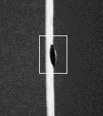
Image processing
- ・ Auto dimension measurement
- ・ Pattern matching technology
- ・ Defect identification / Spatial filtering
- ・ Sub-pixel processing
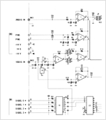
Circuit design
- ・ High-speed
analog/digital signal
processing - ・ High S/N analog circuit
- ・ Power supply circuit
- ・ Various control circuits
LEO Division Handling Systems
| Lifetime Measuring System | To Measure Carrier recombination lifetime. | |
|---|---|---|
| Thin Film evaluation system for FPD |
To process and manage the LTPS and Oxide semiconductor. | |
| Edge/Flatness・ profile Measurement System |
High speed/ High precision measurement of the wafer flatness. | |
| Edge/Makyo System | Micro irregularities on mirror surface can be shown. | |
| Edge/Notch Profile Measurement System |
Possible to auto measure the chamfer width/thickness/edge, wafer diameter, orientation flat length and notch shape. | |
| Edge Roll Off Measuring System | With our unique opical image processing technology, high recision measurement of edge/notch is possible. | |
| Sorting System・ Transfer Machine |
Different combination of measurement menu is available. | |
| Bonding Evaluation・ Edge Defect Inspection System |
Will detect defecrs such as fine scratches along the edge. |

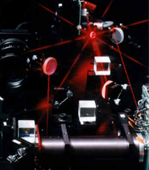
Analysis and measurement of laser/electron/optical technologies.We support cliants in solving their issues with our latest facilities and technologies
![]()
Copyright © KOBELCO research institute All Rights Reserved.