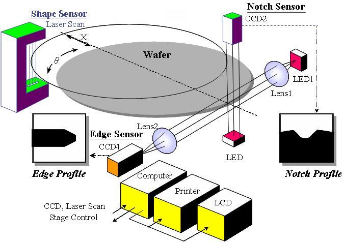
The
structure of edge and notch profiler [LEP-1200] corresponding to 300mm wafers
is shown in the below figure. Since
LEP-1200 measures edge shape, V-notch shape, orientation flat length and wafer
diameter in non-contact method, three types of independent optical sensors (edge
sensor, notch sensor, shape sensor) are equipped.
Wafers are vacuum-adsorbed on the X-theta stage, and the measurement position can be moved to the edge/notch sensor by translation (x)/ rotation (theta) driving. ignals from optics are transferred to the image memory, and image processing is performed by the software installed on the computer. Edge part and orientation flat/ notch shapes are analyzed automatically, and length, angle, radius of curvature, etc. of each part are calculated. Results are indicated and printed by the monitor and printer.
|