|
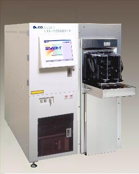
Fully automatic lifetime measurement system with epi/SOI wafer evaluation LTA-2200EP/F |
 |
|
|
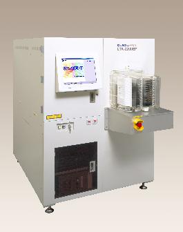
Fully automatic lifetime measurement system with epi/SOI wafer evaluation LTA-2200EP |
 |
|
|
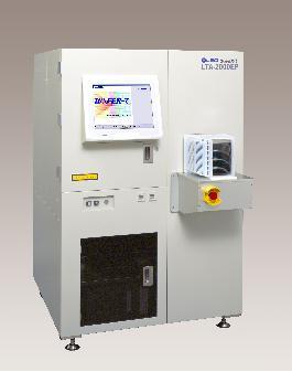
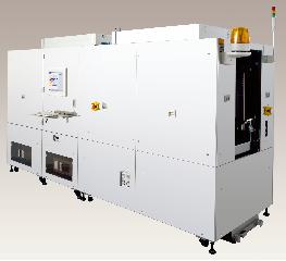
Fully automatic lifetime measurement system with epi/SOI wafer evaluation LTA-2000EP |
 |
|
|
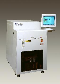
Lifetime measurement system with epi/SOI wafer evaluation LTA-1510EP |
 |
|
|
Evaluation system of low temperature poly silicon LTA-2810SP |
 |
|
|
Evaluation system of low temperature poly silicon and SiC LTA-1800SP |
 |
|
|
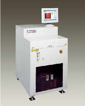
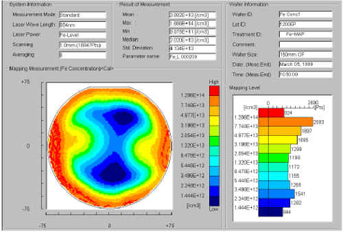
Iron concentration measurement system FE-2000 / FE-2200 |
Example of iron concentration measuring. |
|
|
|||||||||||||||||||||||||||||

|
Corona charge unit CC-2000 / 2200 |
|
|
|
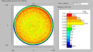
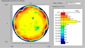 After corona charging tau=250us
| TOP OF PAGE |
|
|
||
| Secondary use of the information, images, etc. provided by this web site is inhibited strictly such as copying, reprinting or selling without approval of the proprietor. Information (contents, images, etc.) in this server may be changed or stopped without prior notice | ||