Examples of observation of silicon wafers


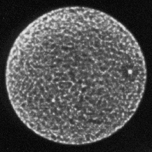
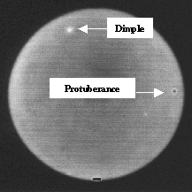
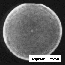
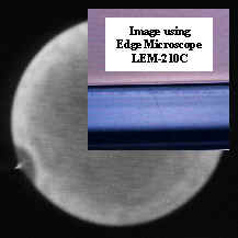
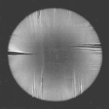
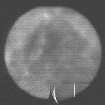
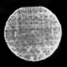
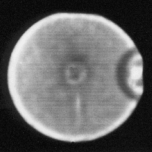
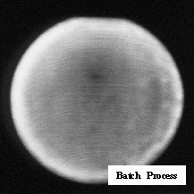
Examples of observation of silicon wafers done by KOBELCO's Makyo system are shown. Surface roughness, protuberance, concave, polishing dent, edge crack and thermal slip are clearly displayed.

Surface roughness

Protuberance/Dimple

Concave


Polishing dent


Polishing dent


Edge crack


Slip dislocation


Slip dislocation


Back side polishing dent


TOP OF PAGE

Kobelco Research Institute, Inc. LEO Division
Sales(Tokyo)/9-12 Kita-Shinagawa, 5-Chome, Shinagawa-ku, TOKYO, 141-8688, JAPAN TEL(03)5739-6820 FAX(03)5739-6393
Sales(Kobe)/5-5 Takatsuka-dai, 1-Chome, Nishi-ku, Kobe, HYOGO, 651-2271, JAPAN TEL(078)992-2985 FAX(078)992-2990
GET FLASH This web site uses FlashPlayer. If not available, Plug-in must be downloaded.
Click the banner
Secondary use of the information, images, etc. provided by this web site is inhibited strictly such as copying, reprinting or selling without approval of the proprietor. Information (contents, images, etc.) in this server may be changed or stopped without prior notice
Copyright(C)Kobelco Research Institute,Inc. All rights reserved.