マテリアル
Materials
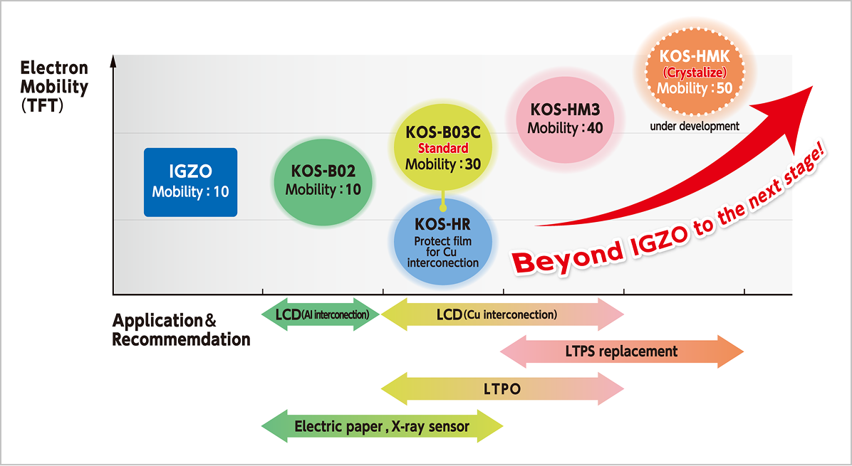
Beyond IGZO to the next stage!
Sputtering Target of High-Mobility Oxide Semiconductor (KOS Series)
~Approaching the solution by adding an additional oxide layer to TFT channel layer~
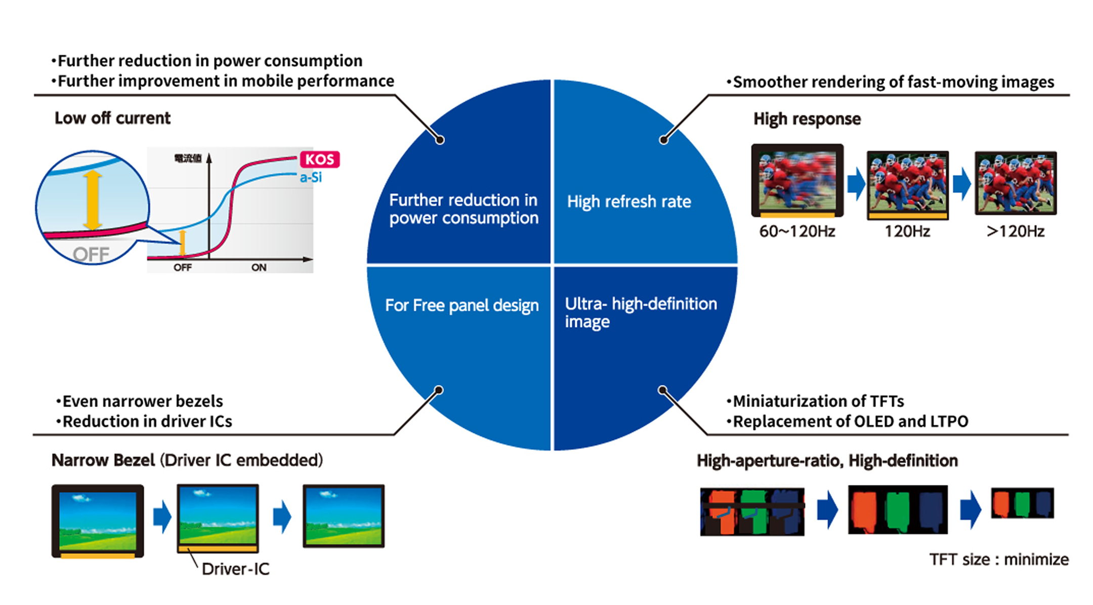
Beyond Point 1
Enhancing IGZO performance to enable high-performance panels!
By depositing high‑mobility oxide thin films, it becomes possible to realize lower power consumption, high refresh rate, greater design flexibility, and ultra‑high‑definition images compared with IGZO, contributing to the increasing diversification of panel requirements.
Beyond Point 2
Advantages of KOS target!
KOS targets are adopted in mass‑production lines and can be provided as sputtering targets compatible with existing production processes.
- Features
-
・Extensive mass production experience for applications such as LCDs, OLEDs, electronic paper, and X-ray sensors.
・Achieves high electron mobility, along with excellent stability and reliability suitable for mass production.
・High mobility performance is maintained even with a stacked structure added to the IGZO layer.
・Offers excellent compatibility with existing LCD and OLED mass production processes, including DC sputtering and low-temperature processing at 350°C.
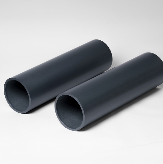
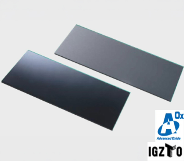
・Targets can be fabricated in a wide range of shapes, including flat plates and cylindrical forms.
Beyond Point 3
Extensive lineup of KOS targets tailored to various application needs!
Based on the industry‑standard KOS‑B03C (Mobility: 30), we offer KOS‑HR for use as a protective film, KOS‑HM3 (Mobility: 40) with higher mobility, and the next‑generation crystalline KOS‑HMK (Mobility: 50, under development) as part of a diverse lineup.
Beyond Point 4
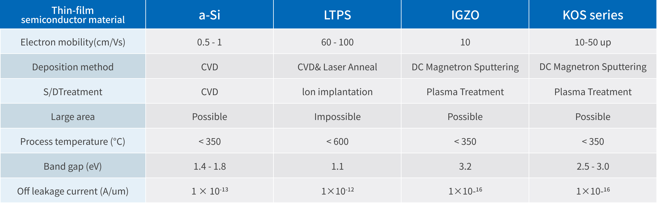
Comparison of Characteristics: a-Si, LTPS, IGZO, and KOS Series.