SYSTEM
Product Lineup
- TOP
- Laser-Electronics-ptics(LEO)
- SYSTEM
- Bonding Evaluation・Edge Defect Inspection System
Bonding Evaluation・Edge Defect Inspection System
Bonding Evaluation Outline
Applying Kobelco Research Institute's existing Technology, it is possible to guide the user through the various evaluation method for wafer bonding process such as TSV, BSI.
Evaluation Content
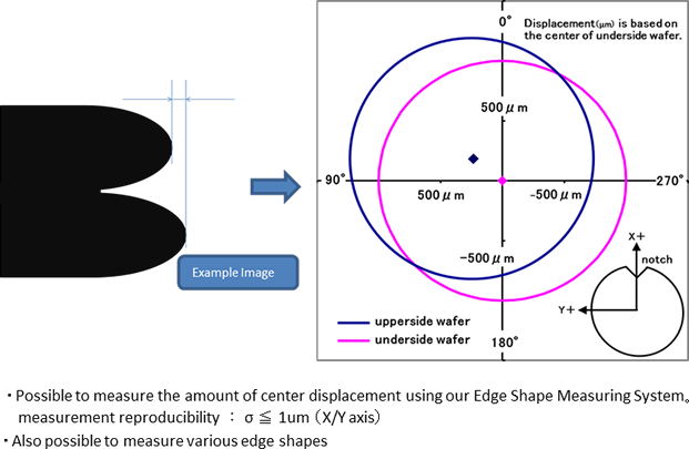
Center Displacement Measurement for Bonding Wafer
Principle
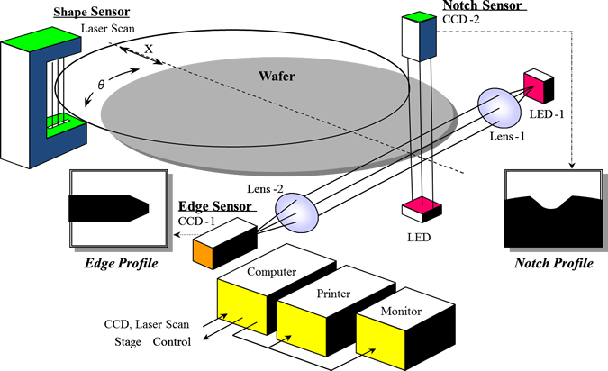
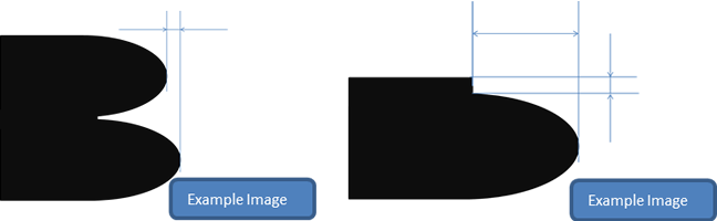
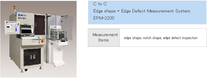
To measure Edge Shape, Notch Shape, Orientation Flat Length, and Wafer Diameter, the system is equipped with 3 independent optical sensor(edge sensor, notch sensor, external shape sensor) .Wafer is vacuum suctioned to a X-θ stage 、and will be able to move the measurement position to edge/notch sensor by translation(X)/rotation(θ)drive.Optical output signal will be transported to image memory. Image processing is performed by software which is installed in the computer.When the image processing is performed, wafer edge, and orientation flat/notch shape is analyzed automatically and each parts length, angle and radius of curvature will be calculated.
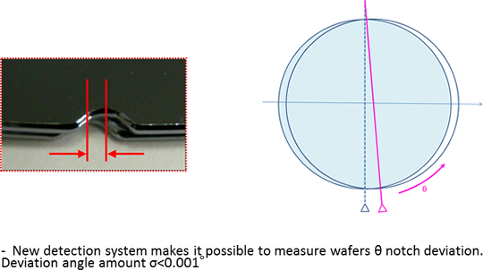
notch deviation Measurement System
Edge Defect Inspection System
System which can automatically detect crack or chipping of the wafer edge .Defect detection of bonded wafer is also possible.Line-camera and Microscope can be selected according to the application.
System Lineup
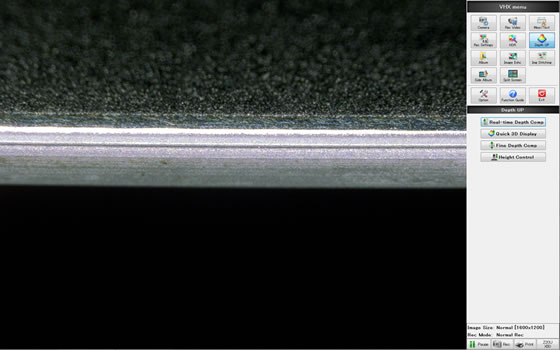
observation example (by microscope)