Laser-Electronics-Optics
(LEO)
- TOP
- Laser-Electronics-Optics(LEO)
Business Overview
We pride ourselves being the expert specifically for Laser Electron, Optics.
-
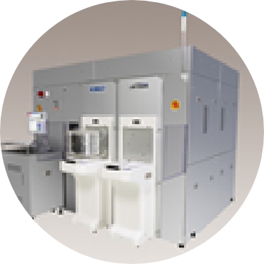
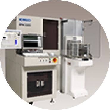
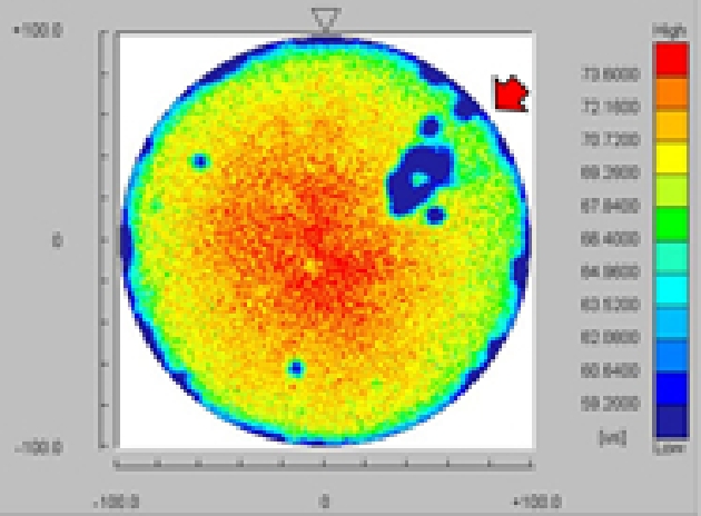
- Flatness・profile Measurement System
-
Broadly used for optimization of wafer edge processing and inspection for shipping.
-
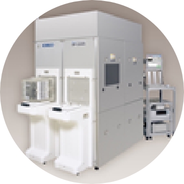
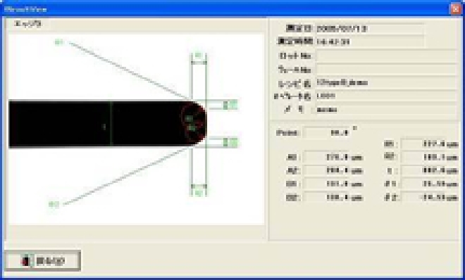
- Edge/Notch Profile Measurement System
-
By our unique optical image processing technology, high precision edge/notch measurement is possible.
-
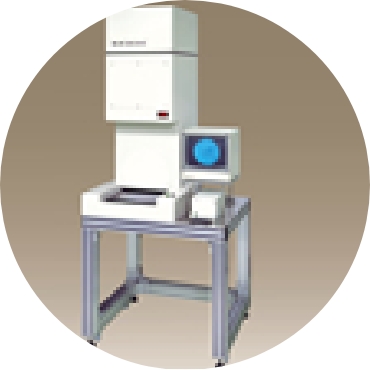
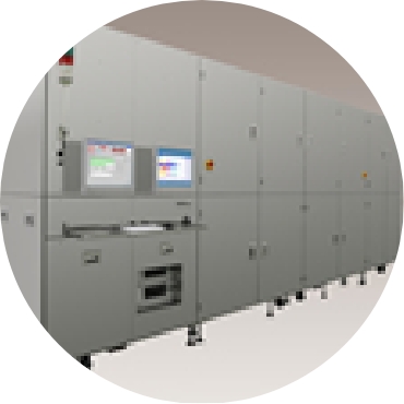
- Makyo System
-
for control of wafer polishing process, delivery inspection and control of heat treatment products.
-
- Bonding Evaluation・Edge Defect Inspection System
-
will detect defects such as fine scratches and cracks near the edge.
-
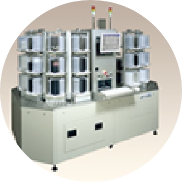
- Sorting System・Transfer Machine
-
Any combination of measurement menu is available.
-
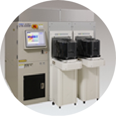
- Lifetime Measuring System
-
Carrier recombination lifetime is measured with system.
-
- Thin Film evaluation system for FPD
-
for valuation of the crystallinity of LTPS without contact and distruction.
-
- Si Semiconductors
-
The time-change of carriers injected into sample by laser will be detected by the reflected power of microwave.
-
- Power Semiconductors
-
Evaluation of various the wide band gap semiconductor is possible.
-
- Application to TSV・BSI field
-
- FPD
-
- LED(Sapphire)
Measurement Services
-
Flatness/Profile Measurement
-
Edge Profile Measurement
-
Makyo Measurement
-
Lifetime Measurement