SYSTEM
Product Lineup
- TOP
- Laser-Electronics-ptics(LEO)
- SYSTEM
- Flatness・profile Measurement System
Flatness・profile Measurement System
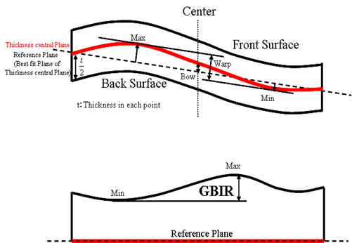
Bow/Warp and Flatness of Wafer
Shape of the wafer are represented by various parameters.Bow and Warp is a parameter representing the shape when the wafer is kept in its natural state without any vacuum suctioning.Bow is the distance between the surface and the best fit plane at the center of an unclamped wafer. Warp is the sum of the maximum positive and negative deviations from the best fit plane(wafer unclamped).GBIR(TTV: total thickness value) is a difference between the maximum and minimum values of the wafer thickness(wafer clamped). GBIR(TTV) can also be obtained by measurement of the front and back surface of wafer when it is at the natural state than calculating using the measurements. SFQR is the evaluation for each site and it is the site flatness index of the reference surface. SFQR is defined when making a cell(for ex, 26mm X 8mm) in any reference plane on the wafer surface. Any dimension on a wafer surface in determined by the least-squares method on the cell surface. SFQR and positive/negative amount from the reference plane it is defined as the range of deviation .
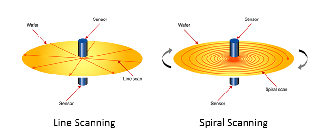
Measurement Method
Possible to suggest two measurement methods upon request.
Sensor Lineup
Upon users request, variety of sensors are available such as capacitance, homodyne interferometer and heterodyne interferometer.
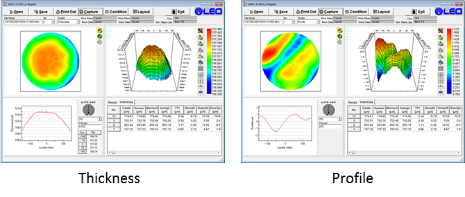
Measuring Example
System Lineup
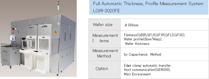
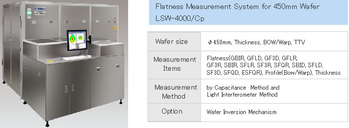
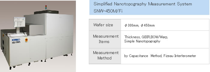
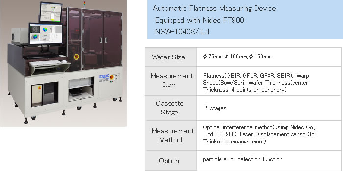
Placement of multiple cassette stage, resistivity meter, PN decision unit could also be done providing a system design with various customers needs.
Option
Resistivity Bias Canceler
During the thickness measurement using the capacitance sensor, RBC(Resistibity Bias Canceler) option is used to solve measurement problem caused by the resistance-resistance uneven stripes.This option is available in all of our systems equipped with the capacitance sensor.
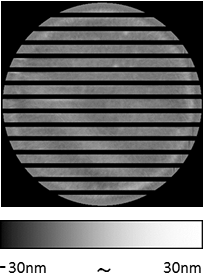
Simplified Nanotopography
By scanning the whole surface using a small interferometer,measurement of microscopic irregularities(Nano-topography) of the wafer up to 450mm is possible in low-cost configuration.
Wafer Inversion Mechanism
Mechanism to rotate wafer(front and rear).
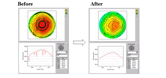
Difference Calculation Software
Data comparison of thickness and profile before and after the wafer process.
Software Modification
With users request software modification such as filtering software for data analysis is available.
Communication function
The devices are possible correspond communication function SECS,GEM of compliance.