Measurement Service List
- TOP
- Laser-Electronics-ptics(LEO)
- Measurement Service List
Measurement Service List
-
Flatness/Profile Measurement
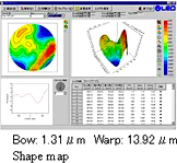
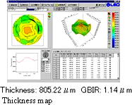
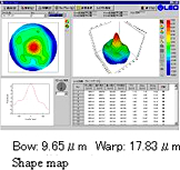
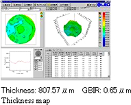
Flatness: Si, SiC Sapphire substrate(Bow, Warp, TTV, GBIR, FSQR, and etc) flatness measurement.
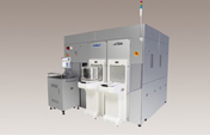
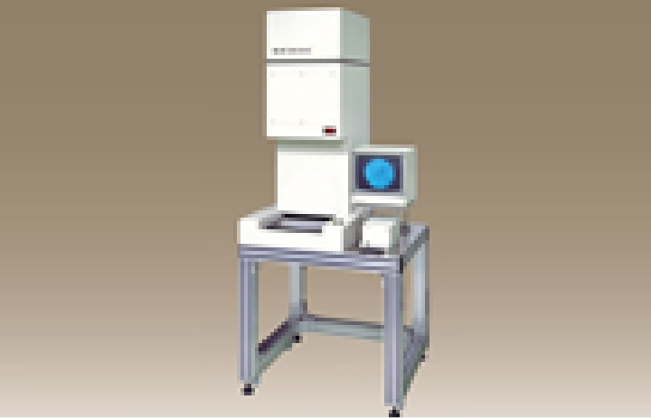
Flatness/Profile Measurement System Detail
Measurement Example


-
Edge Profile Measurement
Edge Profile: Si, SiC, Sapphire Substrate edge(bevel) profile measurement.
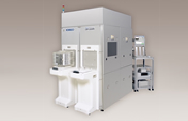
Edge/Notch shape measuring system details
Edge/Notch profile mearement example
shows the measurement example of edge/notch profile.
different profiles canbe supported using optional software.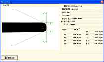
dge profile measurement example(LCD display) 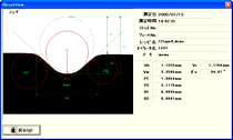
Edge profile measurement example(LCD display) 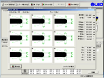
Edge 9 points display screen
-
Makyo Observation
Makyo: Si Substrate(Mirror) surface observation
Si Wafer surface observation example
Surface Roughness, Projection, Dent, Grinding Masks , Edge Crack, and Thermal Slip appears clearly
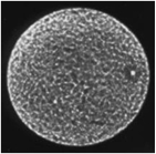
面荒れ
Orange Peel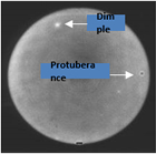
突起/凹み
Dimple/Protuberance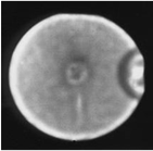
凹み
Dimple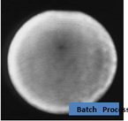
研磨痕
Polish Mark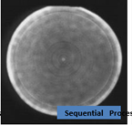
研磨痕
Polish Mark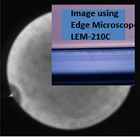
エッジクラック
Edge Crack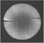
スリップ転位
Thermal Slip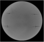
スリップ転位
Thermal Slip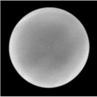
研削痕
Grinding
-
Lifetime Measurement
Lifetime measurment for Semiconductor materials such as Si,SiC, GaN, LTPS, and IGZO
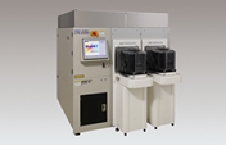
Lifetime Measurement System detail
Lifetime mapping example of bulk wafer
Lifetime measurement for semiconductor materials such asn Si, SiC, GaN, LTPS, and IGZO. By measuring the lifetime, the heavy metal mixture of a wafers, the integrity of the crystals can be measured and also the wafer pollution cause may be detected.
Standard Spec. pitch measurement of our Lifetime equipment is 0.5mm and with it high speed small mapping is possible.
Blue figure represents short lifetime.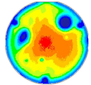
contamination by chucking 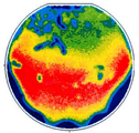
contamination by oxidation boat 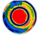
OSF (Oxidation-induced Stacking Fault) ring 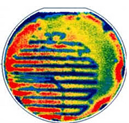
Pin contact from the manufacturing equipment 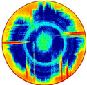
Slip Dslocation by thermal treatment 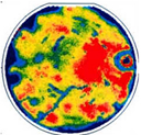
Absorption traces of vacuum tweezers