LEO Business Overview
- TOP
- Laser-Electronics-ptics(LEO)
- LEO Business Overview
Outline of KOBELCO RESEARCH INSTITUTE, INC.
| Name | KOBELCO RESEARCH INSTITUTE, INC. | |
| office | Head Office |
Kokusai Kenko Kaihatsu Center 3F 1-5-1 Wakihamakaigandori, Chuo-ku, Kobe, HYOGO, 651-0073, JAPAN TEL : 81-78-272-5915 FAX : 81-78-265-3622 MAP |
|---|---|---|
| Sales(Tokyo) |
5-9-12 Kitashinagawa, Shinagawa-ku, TOKYO, 141-8688, JAPAN TEL : 81-3-5739-5363 FAX : 81-3-5739-5371 MAP |
|
| Sales(Kobe) |
5-5 Takatsuka-dai, 1-Chome, Nishi-ku, Kobe, HYOGO, 651-2271, JAPAN TEL : 81-78-992-2985 FAX : 81-78-992-2990 MAP |
|
| Establishment | June 1979 | |
| Services |
Material mechanical and physical property evaluation, Corrosion resistance evaluation, Corrosion trouble examination, Micro surface and fine area analysis study, Chemical analysis, Organic analysis, Physical analysis, Corrosion test, Property test, Strength test, Welding test, Environment measurement analysis and test, Spattering target materials, parts, test materials Semiconductor evaluation products (New: LEO Division) |
|
| Major customers | Kobe steel, Ltd., Kobe Steel Group companies, Public agencies, Power companies, Electric equipment companies, Automobile companies, Others | |
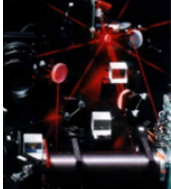
History of LEO Division

LEO Division of KOBELCO RESEARCH INSTITUTE, INC. carried on the business of LEO Giken, special group centered on Laser-Electro-Optics: LEO. KOBELCO has produced numerous products focusing on L-E-O technologies such as lifetime measuring unit, ion dose monitor, edge profile monitor and wafer sorter, and has been satisfying customers' needs with high technology and accumulated experiences. We pride ourselves on placing our "First priority on customers".
Products treated by LEO Division
A central role in the test and evaluation field in the future is taken by KOBELCO, by making the most use of our elemental technologies accumulated over long time.
-
Optical design
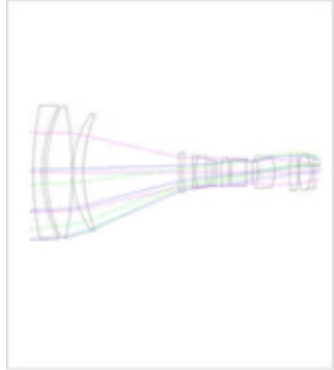 ・ Optical simulation
・ Modulation/deflection system
・ Interference,
convergence system
・ Laser scanning -
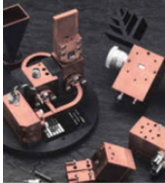
Fine mechanics
 ・ High-precision transfer
・ Wafer handling mechanism with edge grip
・ Anti-oscillation technology
・ Mechanical control software -
CCD application
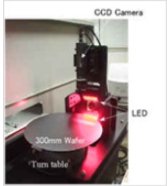 ・ Super high resolution image input by line sensor
・ Real time image correction
・ High dynamic range image sensing
・ High intensity light source -
Microwave circuit
 ・ High sensitivity antenna detecting carrier density
・ Reflected noise control technology
・ Differential detection technology -
Precise photo-measurement
 ・ Homodyne interference system
・ Heterodyne interference system
・ High sensitivity oscillation measurement
・ Precise position measurement -
Image processing
 ・ Auto dimension measurement
・ Pattern matching technology
・ Defect identification / Spatial filtering
・ Sub-pixel processing
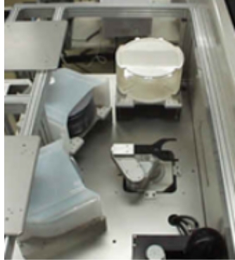
LEO Division Handling Systems
-
Edge/Flatness・profile Measurement System
High speed/ High precision measurement of the wafer flatness.
-
Edge/Notch Profile Measurement System
Possible to auto measure the chamfer width/thickness/edge, wafer diameter, orientation flat length and notch shape.
-
Edge/Makyo System
Micro irregularities on mirror surface can be shown.
-
Bonding Evaluation・Edge Defect Inspection System
Will detect defecrs such as fine scratches along the edge.
-
Sorting System・Transfer Machine
Different combination of measurement menu is available.
-
Lifetime Measuring System
To Measure Carrier recombination lifetime.
-
Thin Film evaluation system for FPD
To process and manage the LTPS and Oxide semiconductor.